EDGED TENSOR PROCESSING
CORES
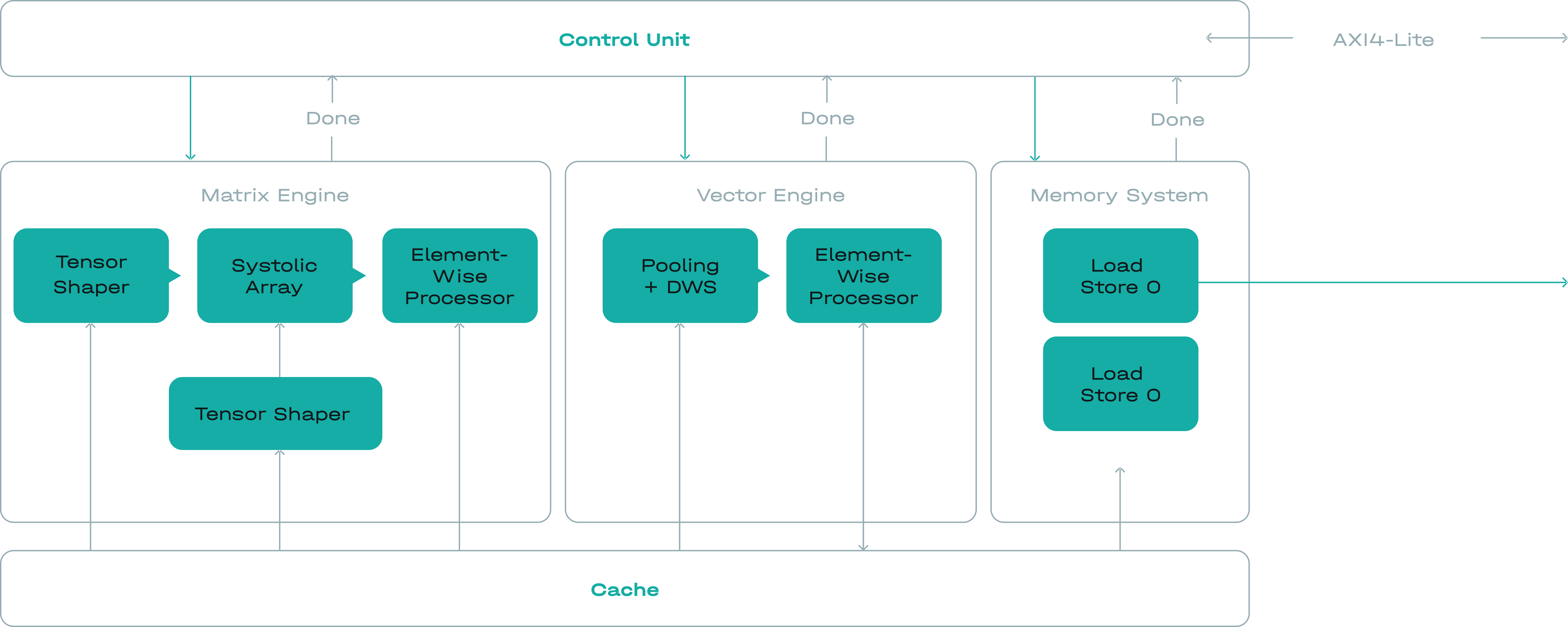
EDGED has taken a new architectural approach to accelerating neural networks. Instead of creating a small programmable core and replicating it dozens or hundreds of times (such as e.g. Graphcore), we designed a single computation block with matrix and vector operations units.

BENEFITS
Fully parametric
Our IP is fully parametric, which means that it can be easily adapted to different performance and power consumption characteristics. We have a tiny footprint version for FD-SOI, high-performance versions for FinFET, and anything in between.
Low-latency
Combined with our proprietary neural network quantization utility and compiler, our IP provides the best gate count and frequency inference latency. This makes us ideal for edge applications that require a fast response time such as ADAS, industrial security, etc.
Silicon-tested
Unlike so many other vendors jumping on the AI bandwagon, we have a working chip in our hands. Our reference chip has been already installed in field applications, outrunning industry leaders, and commended in a Linley Group report.
Geeky details
Our approach greatly reduces instruction-decoding overhead, enabling the Tensor Processor Unit (TPU) to pack frequently used data in SRAM to minimise usage inefficient external memory while computing more than 16 000 multiplyaccumulate (MAC) operations per cycle. The result is performance of up to 50 trillion operations per second (TOPS). The internal vector engine can also handle floating-point data, allowing it to perform RNN and mixed precision calculations.
Normally NN acceleration requires a tradeoff between minimum latency and maximum performance. When even just a small percentage of the workload requires milliseconds responses, a traditional GPU’s performance quickly degrades. This means deploying more racks, more power, and more maintenance costs, excessive power consumption. With EDGE TPU, there is no tradeoff. Responsiveness and performance go hand in hand, providing agility and enables high performance in restricted power supply applications.
EDGED TPU FAMILY FOR INFERENCE
EDGED TPU IP Core Customizable IP block of tensor accelerator, suitable for manufacturing in data systems
REFERENCE DESIGN CHIP H Processor for high performance low latency processing systems
REFERENCE DESIGN CHIP E System on a chip for embedded systems with general purpose processor and EDGED TPU
OUR SOLUTIONS
Best in class chip performance @28nm, TPU of 40 TOPS, energy efficiency of 2 TOPS per Watt
Best in class throughput on given latency
Seamless compatibility with popular open source NN frameworks/libraries, such as TensorFlow, Keras, ONNX
Optional h/w support of recurrent DNN (LSTM, GRU)
28nm Silicon-proven architectures and design
APPLICATION SCOPE
Self-driving, unmanned vehicles and robotic control systems
Automatic guidance systems
Pattern recognition systems
Decision support systems (pattern recognition, forecasting, risk assessment, etc.)
Voice recognition and speech-to-text conversion, speech synthesis, keyword spotting
Image enhancement
Identification of abnormal situations in complex systems
Dark data based forecasting
EDGED TPU IP CORE
Fully parametric character IP block of EDGED TPU make possible deep optimization of performance per square nm and performance per watt characteristics based on customer’s specific computational requirements, i.e. neural network topology and application specific requirements (bandwidth & latency)
Silicon-proven architectures and design @28nm HPC+.
Linley Microprocessor Report available.
Conv layers
Fully-connected, Convolution (2d/3d, Depth-wise separable, Dilated conv, Deconv)
RNNs
LSTM, GRU
ReLU-based functions
ReLU, Leaky ReLU (PReLU), ReLU6, HardTanh
Non-ReLU-based functions
Sigmoid, Tanh, SoftMax
Pooling modes
Average, Max
Other
Residual (Skip-connections), Attention, Concatenation
Tensor Transforms
Depth2Space, Space2Depth, Transpose
REFERENCE CHIP H
EDGED reference design chip H is a processor for low latency high intensity inference with PCIe host processor interface. Reference implementation is presented by a PCIe board. A typical solution for cloud is presented by a PCIe expansion board compatible with the weight and size specifications of server rack solutions. Sample board with EDGED TPU with PCIe-card form factor (half-length, half-height)
Number of cores
>16.000
Clock rate
1000 MHZ (variable)
Technology
28 nm HPC+
Power
Max. 50 W

REFERENCE CHIP E
EDGED TPU E is on reference SoC for embedded applications with a dual-core superscalar microprocessor, tensor accelerator EDGED TPU and a large set of interfaces for connecting external devices.
